
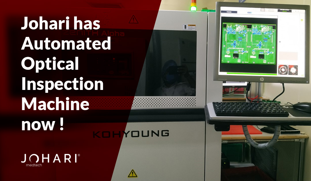
We are delighted to share the addition of a new asset in our manufacturing facility, Automated optical Inspection Machine. This new member in our manufacturing capability portfolio shall boost productivity four folds and improve the accuracy, speed, and efficiency of PCB manufacturing.
How will AOI improve the efficiency of PCB inspection?
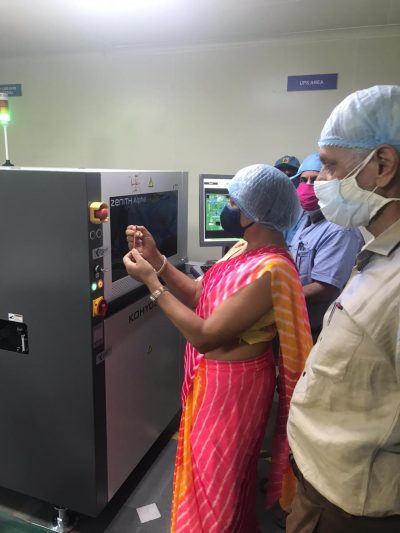
As medical devices are becoming more compact day by day PCBs are becoming compact & small. Manual inspection is a very complex task in such a scenario. The chances of errors are high in manual inspection & it might lead to a bigger fault while assembly or testing. The market requires high volume, quality, and innovative devices therefore it’s extremely important to minimize errors in the first place. AOI has integrated electronic test strategy to ensure cost-optimized, fast, and zero error inspection. AOI systems are kept next to the soldering process to ensure proper inspection.
Basics of Automatic Optical Inspection
The automated optical inspection machine inspects the PCB for:
- Scratches
- Nodules
- Stains
- Dimension Defects [thinning of solder, shorts, and open circuits].
- Incorrect components
- Missing component
- Component placing defect
How does this work?
The board is visually scanned by the light source by a high-definition camera which captures the deformities. Then, the picture captured is compared with standard PCB info in the database of the machine.
There are many ways in which the AOI detects the defects in the board:
- Template Matching
- Pattern Matching
- Statistical Pattern Matching
AOI implements a sophisticated Manufacturing environment ensuring 100% accuracy with zero defects in the PCB.
What is the light source of AOI?
Lightning forms the key element of AOI. There are multiple illuminations present to correctly identify, analyze and map errors. Every illumination has a different role to play for a different product PCB. Some commonly used lighting systems in the AOI are:
- Fluorescent Lighting System
- LED lighting
- Infrared or Ultraviolet Lightning
Way forward…
Gradually we are exploring many dimensions in the manufacturing segment. Diagnostics, Life sciences, Electrotherapy, Biochemistry, Microbiology, and so on. All these equipment and devices require 100% efficiency in processes. Also, as the medical technologies are becoming compact, their PCB manufacturing is becoming more intricate. It’s important to have quality manufacturing to ensure safety, durability and market viability of the product. We keep adding newer capability to remain relevant in the volatile times of medical device manufacturing.